Home
 |
 |
 |
 |
This wiki describes how to order and build the Hillside family of split ergonomic keyboards. See the repo readme for the Hillside features, firmware access and rationale. Hillside is provided as KiCad files, zips of the files for ordering the PCB, build documentation, and QMK and ZMK firmware files.
Building a Hillside involves some soldering skills and tools, having the PCBs created, ordering parts, and assembly. For the Hillside 46, the factory can solder the SMT parts.
You need decent small electronics soldering skills and a temperature controlled iron. The through-hole parts are easy with good soldering technique. The SMT parts require a more careful touch but are the larger and easier SMT sizes. See Soldering Skills and Tools for some useful guides and videos. A bad solder job will increase your frustration and likely require debugging. A good clean solder job is likely to lead to a trouble-free assembly.
The PCB gerber and drill files to send to a PCB manufacturer are under releases and in the commits history. If you would like to make changes to the boards, the KiCad files are in the specific board directories here.
See Ordering Hillside 46.
Upload to a PCB manufacturer the latest release of that board's gerber files. I have used both JLCPCB and AllPCB with settings of: 10mil trace, 0.4mm min drill hole/via size, 2 layers, 1.6mm board, 1oz copper. See the board details for the PCB size.
One thing that the fab might ask about is within the encoder footprint along the bottom of the board. That footprint handles either a choc switch or an encoder. Yet the choc switch's right stabilizer hole is right next to the ground pin hole for the encoder. If the stabilizer hole was the normal non-plated through-hole, they likely would complain that the two were too close. So the stabilizer hole is described as a plated though-hole and there is a note in the readme within the gerber folder describing that it is fine if it joins with the adjacent plated through-hole ground pin for the encoder. But they may not read that note and may ask about it.
The fabrication cost is around $11 plus $13 to $27 shipping (for five PCBs or two and a half keyboards) for a board with a simple solder mask and finish.
The core parts for the board are MCUs and sockets, diodes, TRRS jacks, switches and keys. See Parts for the details.
For options such as tenting, encoders, haptic feedback or a trackball, see Tenting, Case and Optional Parts.
For a wireless Nice!nano build, you will also need a battery, power switch, and a capacitor; see Wireless Nicenano Parts.
It is highly recommended that you read through all the preparation and build pages before starting work.
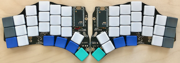
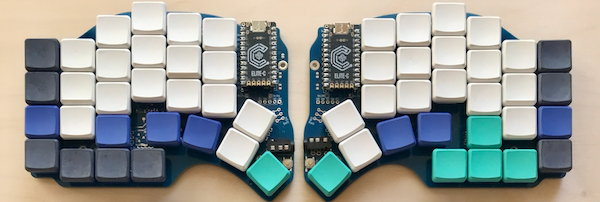
Building your board differs very little between the Hillside models. It differs mainly in the number of diodes, switches and keys and their locations. The build guide images were created for the Hillside 48, but the required steps are the same for all Hillside boards.
The build links to the right will step you through constructing your board.
You will be fine if you place all components on the top of the board. But they don't all need to be on the top. Specifically:
- The side you type on is the top. The key switches go on the top.
- The MCU goes on the top. In terms of the orientation of the MCU, look at the "Match with MCU labels" arrows on the top side of the PCB and match those holes to the pin labels on your MCU. This usually means the smooth, component free, side of the MCU will face up and the component filled side down. But check the pin labels on your MCU. You solder on the bottom, but do not match to the labels on the bottom side of the PCB.
- The diodes, capacitors, resistors and ESD chip can go on the top or bottom.
- The reset, TRRS and battery switch make more sense on top for access and height, though electrically either side is fine.
- The LEDs go on the top facing down. To work electrically, they need to shine through the hole in the PCB and be oriented with the ground pin. You could put them on the bottom and shining up if you wanted.
(You could put the MCU on the bottom. It is the same as thinking about putting the MCU on the top and the key switches on the bottom. Just match the hole labels on the bottom side then. This will generally mean the component rich side of the MCU faces the PCB.)