::ATTENTION::
-  Due to the changes in ANT's EBL process, the coupling angles for *ebeam_gc_te1550* and *ebeam_gc_tm1550* components may be impacted.
- There is no change in the coupling angles when fabricating the components with UW's EBL process. - SiEPIC EBeam PDK, Library - for silicon photonics layout, design, verification and circuit simulation
- by Lukas Chrostowski (lukasc-ubc), (c) 2015-2022, with contributions by: Zeqin Lu, Jaspreet Jhoja, Xu Wang, Jonas Flueckiger, Brett Poulsen (bpoulse).
- Package in KLayout, klayout.de (version 0.27 +)
- Instruction on design, layout, fabrication, test, data analysis for silicon photonics provided in the edX course: Silicon Photonics Design, Fabrication and Data Analysis and textbook Silicon Photonics Design: From Devices to Systems by Lukas Chrostowski and Michael Hochberg.
- Fabrication runs via Electron Beam Lithography are available, including openEBL fabrication, and Applied Nanotools NanoSOI.
- Citing this work: Lukas Chrostowski, Zeqin Lu, Jonas Flueckiger, Xu Wang, Jackson Klein, Amy Liu, Jaspreet Jhoja, James Pond, "Design and simulation of silicon photonic schematics and layouts," Proc. SPIE 9891, Silicon Photonics and Photonic Integrated Circuits V, 989114 (May 13, 2016); doi:10.1117/12.2230376.
- Details are provided in the Wiki page: Installation instructions. KLayout's package manager is used for both downloading and installing the package.
- Use an open-source layout tool (KLayout) to implement a sophisticated layout design environment for silicon photonics
- Support for both GUI and script-based layout, or combinations of both.
- KLayout-INTERCONNECT integration offers a layout-first design methodology. Inspired by Layout Versus Schematic tools, this PDK includes netlist extraction routines to generate a schematic from the layout. This allows the user to directly simulate from the layout, without needing to create the schematic first. This approach is possibly more appealing to photonics designers who are accustomed to designing physical layouts, rather than schematics. A library of components (layout and compact models) is included in the Process Design Kit, specifically for silicon photonics fabrication via Electron Beam Lithography.
- Whereas a typical schematic-driven design flow includes a schematic, circuit simulation, layout, and verification (see Chapter 10 of the textbook), the approach taken here is Layout-driven, followed by verification, then a schematic (via a netlist extraction) and simulations.
- Read more details in our two SPIE papers: Design and simulation of silicon photonic schematics and layouts and Schematic Driven Silicon Photonics Design.
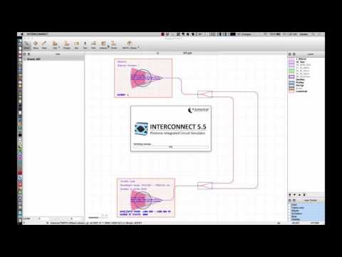
Video of a layout and simulation of a ring resonator circuit:
Monte Carlo simulations of a ring resonator circuit, showing fabrication variations:
Layout of a Mach-Zehnder Interferometer:
Simulations for the MZI:
- Process Design Kit (PDK): this package, including fabrication documentation, scripts, etc.
- EBeam Layer definitions for KLayout (klayout_Layers_EBeam.lyp).
- PCells: directional couplers, ring resonator, taper, Bragg grating
- Sample scripts to create a layout, including waveguide generation functions: Mach-Zehnder Interferometer test structures; Ring resonator test structure.
- GDS Library, updated with marker layers for verification/netlist generation.
- Verification:
- Scanning the layout. Finding waveguides, devices, pins.
- Verification: Identifying if there are missing connections, mismatched waveguides, too few points in a bend, etc.
- Example layouts using the library for verification (EBeam_LukasChrostowski_E_LVS.gds, SiEPIC_EBeam_PDK_Verification_Check.gds).
- Verification for automated measurements
- Circuit simulations:
- Netlist generation
- Creating a Spice netlist suitable for for circuit simulations. This includes extracting the waveguide length (wg_length) for all waveguides.
- Menu item "Lumerical INTERCONNECT" will automatically: generate the netlist, launch Lumerical INTERCONNECT to perform the circuit simulations, and pop-up a plot of the transmission spectrum.
- Monte Carlo simulations, including waveguides, ring resonators built using directional couplers, y-branches, grating couplers.
- Waveguide functionality:
- Hot Key "W": selected paths are first snapped to the nearest pins, then converted to waveguides.
- Hot Key "Shift-W": selected waveguides are converted back to paths.
- Hot Key "Ctrl-Shift-W": measure the length of the selected waveguides.
- Hot Key "Ctrl-Shift-R": resize the waveguides, for a given target length.
- Layout object snapping
- Hot Key "Shift-O": Snaps the selected object to the one where the mouse is hovering over.
You can download the latest development version (master) of the PDK: Zip file download of the PDK
It is posted on GitHub for 1) revision control, 2) so that others can contribute to it, find bugs, 3) easy download of the latest version.
To contribute to the PDK:
- On the GitHub web page, Fork a copy of the project into your own account.
- Clone to your Desktop
- Make edits/contributions. You can use the KLayout IDE to write Python (or Ruby) scripts; KLayout Python IDE for writing/debugging PCells/scripts/macros.
- "Commit to master" (your own master)
- Create a Pull Request -- this will notify me of your contribution, which I can merge into the main project
I am personally using GitHub desktop to synchronize my files. Then I created symbolic links in my .klayout folder to point to the local copy of this repository. This is useful to automatically update my local KLayout installation (e.g., multiple computers), as changes are made in GitHub.


