![]()
![]()
![]()
A 2-trit async balanced ternary calculator allowing multiplication, addition and subtraction with negative numbers in binary encoded ternary

This chip is a 2-trit asynchronous balanced ternary calculator having 2 functions: multiplication and addition/subtraction (which is one function in balanced ternary). It demonstrates how to build ternary logic with binary transistors using binary encoded ternary (BET). 1-trit (3 values) is thus encoded in 2-bits (4 values, 1 is ignored). This inefficient encoding is neccesary since current CMOS processes can only construct binary transistors. Despite this inefficiency, there are several benefits on various levels. We use balanced ternary notation meaning that each trit contains -1, 0 and +1. This allows balanced arithmethic with negative numbers without any special circuitry or convention (eg. 2's complement). Typically designing ternary logic is cumbersome. The open source tool MRCS works with binary and ternary and mixed truth tables (TT) that automatically convert to netlist and verilog. This means a designer does not need to think in binary when making ternary logic. The design can be verified 1) manually in the tool, 2) automated by uploading a CSV with TT input-output pairs, 3) by using Vivado verilog simulator (test bench is included), 4) by deploying on FPGA (constraint file for Xilinx Basys3 is included) or 5) by using HSPICE for analog verification. The HSPICE verification is currently using 3 types of carbon nanotubes transistors (CNTFET) as technology as these are designed for ternary signals. Future versions of MRCS will integrate the various SPICE libs from the Sky130 open PDK.
- balanced ternary multiplication
- balanced ternary addition/subtraction
- Load MRCS WebGL or build Standalone (Unity C# Project)
- Click "Import component" and select the src/MRCS/MRCS_Export_TT03-BTCalculator.zip package from this repo
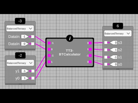
- Drag and drop the chip on the canvas and click on the inputs to see the computations being done in real-time.
- To verify in MRCS, open the chip such that the inputs and outputs are visible. Click verify and upload the src/Tests/test_tt03-btcalculator.csv. Wait a few minutes to see a verification result screen.
- Install Vivado ML Free, See instructions
- Install FPGA Board eg. for Basys3, manual of Basys3
- Create new project, choose FPGA board (eg. Basys3) and set top module name to c_TT3_BTCalculator
- Add design source, select /src/c_TT03_BTCalculator.v
- Add simulation source, select /src/c_TT03_BTCalculator_tb.v
- Add constraints, select /src/Basys3_FPGA/basys3_constraints_8x8.xdc
- Run simulation. Confirming that input-output result is 55->96 and 79->db
- Run synthesis.
- Run implementation.
- Generate bitstream and program
- Optional: flash the chip permanently by following these instructions


The two truthtables of the BTA. Note that the input B is 0 and input A is 1 and output is 1 (0+1=1). The truthtable cell becomes more yellow and finally red when the state is used more.

The discrete CNTFET transistor implementation of 7PB (SUM) generated by MRCS. Transistors that are greyed-out are not conducting with given input. Visible is that a single transistor path is active (in this case actually 2!), thus connecting output to VDD resulting in output 1 and reflecting the truth table state.

2do add HSPICE sim of the 7PB


MRCS allows binary and ternary truth tables. Both balanced {-1,0,1} and unbalanced {0,1,2} ternary is allowed. The key thing to realize is that balanced and unbalanced ternary is only a semantic interpretation. Physically they are the same signals. Binary is just the extreme sides of them. So for balanced ternary logical -1 is 0 Volt, logical 0 is VDD/2 and logical 1 is VDD. In the case of binary logical 0 = 0 Volt and logical 1 is VDD. In the case of unbalanced ternary the logical 0 is 0 Volt, logical 1 is VDD/2 and logical 2 is VDD. This interpretation scheme works for single power supply circuit. In the case of dual power supply, at the expense of additional power routing (and resulting in several benefits) the interpretation scheme for balanced ternary becomes logical -1 is -VDD, logical 0 is 0 Volt (actively driven!) and logical 1 is VDD. For Binary it becomes logical 0 is -VDD and logical 1 is VDD. With this interpreting binary in a ternary signal is simple, it is always the extremes.
We use the following binary encoded ternary (bet) scheme:
- Logical -1 = 2'b01 (first bit is MSB)
- Logical 0 = 2'b11
- Logical 1 = 2'b10
- illegal = 2'b00
The reason for this scheme is that a 1bit DAC implemented with a differential opamp can interpret logical -1 and logical 1 since there is a difference signal. In addition, this scheme allows binary synthesis tools such as ABC to optimize the 2'b00 state. If the circuit is in that state, we know there is an issue. Finally, since all transitions are single bit changes (with 3 states, a property due to balanced ternary arithmethic) power consumption is low. Normally with binary arithmetic, to process negative numbers all bits need to be flipped (inverted) plus one (2's complement conversion) followed by a regular ADD operation.
In pictures, the inputs and outputs are automatically converted by MRCS from ternary to binary. Below is a 4 trit to 8 bit conversion as used in this chip. For example x1 is a logical -1 and is encoded as 2'b01.

The truth table functions are automatically converted from ternary to binary. For example the balanced ternary standard inverter, STI or heptavintimal index 5 is converted to binary encoded ternary as follows:

For this image you still have to imagine that the ternary input signal logical 0 is actually encoded as 2'b11. The generated verilog for this function looks like this:
module c_STI (
     input [1:0] io_in,
     output [1:0] io_out
);

wire [1:0] tnet_0 = io_in[1:0]; //in

wire [1:0] tnet_1;

assign io_out[1:0] = tnet_1; //out

f_5_bet LogicGate_0 (
.portA(tnet_0),
.out(tnet_1)
);

endmodule

module f_5_bet (
     input wire[1:0] portA,
     output wire[1:0] out
     );

     assign out =
    (portA == 2'b01) ? 2'b10 :
    (portA == 2'b10) ? 2'b01 :
     2'b11;
endmoduleTinyTapeout is an educational project that aims to make it easier and cheaper than ever to get your digital designs manufactured on a real chip!
Go to https://tinytapeout.com for instructions!
Edit the info.yaml and change the wokwi_id to match your project.
Please see the instructions for:
When you edit the info.yaml to choose a different ID, the GitHub Action will fetch the digital netlist of your design from Wokwi.
After that, the action uses the open source ASIC tool called OpenLane to build the files needed to fabricate an ASIC.
- Share your GDS on Twitter, tag it #tinytapeout and link me!