HowTheMinimigCoreWorks
This document tries to describe the inner workings of the Minimig. This document is for developers porting or altering the Minimig.
This document is not for you if you don't know what the minimig is or how to use it. In that case a good starting point would be the Wikipedia entry for the Minimig or the Minimig forum.
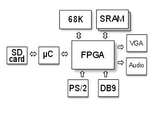
The original Minimig consists of very few components as depicted above. These are:
- 68k CPU
- This is the heart of the device. It's the CPU executing the Amiga software in exact the same way it would do in a real Amiga.
- FPGA
- This is the part doing most of the work all other chips besides the 68k CPU would do in a real Amiga.
- 2 x 1MB SRAM
- This is used as Amiga main memory as well as ROM replacement for the kickstart
- PS/2
- The FPGA contains a converter from PS/2 to amiga mouse and keyboard, so the 68k doesn't see the ps/2 but instead accepts it as a standard amiga mouse and keybord
- DB9
- The DB9 connectors accept genuine Amiga DB9 joysticks.
- VGA
- The VGA output can output an Amiga compatible PAL RGB signal. Additional logic inside the FPGA can double each line for output and thus creating a signal that is accepted by VGA displays that can cope with 50 Hz PAL vsync frequency.
- Audio
- Audio is generated via a simple 2 x 1 bit audio output which is driven directly by the FPGA using a sigmal delta converter.
- Microcontroller
- The microcontroller has two main purposes: It configures the FPGA + SRAM and while the system is running and it acts as a floppy disk emulator and general system controller. In the original minimig this is a PIC. A more powerful ARM based replacement is available as an update.
- SD card
- The SD card contains the FPGA configuration, the ROM images and optionally floppy disk images
Only one component in the minimig has permanent memory: The Microcontroller. It's the only component that knows what to do on power-on. The microcontrollers permanent code memory needs to be filled with its firmware either by placing it into a separate flash programming device (PIC), or by using some special upload cable directly in the target circuit or via an on-board USB programming nterface (ARM). Once the microcontroller has been programmed this way it may be able to update itself e.g. from SD card. This depends on the type of microcontroller and needs to be supported by the firmware installed on the microcontroller. Only the ARM controller supports this.
The microcontroller has direct access to the SD card. This is the only component the microcontroller initially has access to as the FPGA does not provide any functionality in it's unconfigured state after power-on. The only thing it's able to do is to accept some configuration via a special interface. The microcontroller is connected to this interface. It reads a FPGA configuration file from SD card (minimig.bin) and uses this to configure the FPGA. The FPGA afterwards provides the functionality of the entire Amiga except the 68k CPU. The FPGA configuration also includes helper functionality to e.g. connect a PS/2 mouse or to enable communication with the microcontroller while the system is running or to display a video overlay to control the amiga (e.g. select disk images from the SD card for floppy disk emulation) or to change hardware settings like the RAM size. Also the microcontroller has a rs232 interface allowing it to output debug and status information while the FPGA is not configured.
The FPGA configuration also includes a minimal 68k code block (bootrom). The bootrom is overlayed over some of the RAM after FPGA configuration and is executed by the 68k immediately after the FPGA is configured.
The bootrom has a counterpart in the microcontrollers code. Both parts are communicating via messages sent through the floppy disk read buffer. The bootrom issues disk read accesses for floppy 1. The microcontroller responds with some magic command pattern which it returns instead of actual floppy disk data. These command messages are used to upload the kickstart rom code from sd card into RAM, to display text on the boot screen, to clear memory or to leave the boot state and to disable the bootrom.
Once the kickstart ROM is in place the bootrom is disabled and the 68k CPU is being reset to start executing the kickstart rom code from sram. At this moment the 68k CPU starts doing exactly what a real Amiga would do after power-on.
The Micrcontroller is connected to the FPGA via SPI. The SPI master is the microcontroller and the SPI slave is the FPGA. While the SPI bus is fully visible to the microcontroller it's nearly invisible to the amiga. Instead the microcontroller interacts with the various amiga peripherals inside the FPGA and reacts on them in order to change settings like the video mode or to deliver floppy disk image contents to the floppy disk controller, but also to control the on screen display overlay (OSD).
Three chip select lines are used between the microcontroller and the FPGA. Only two if these (CS0 and CS1) are being used directly. CS0 selects the amiga FDD and HDD emulation inside the FPGA and CS1 selects the OSD and OSD related control functions. CS2 is used in a very special way as it is used during SD card read accesses which are controlled by the microcontroller but the data transferred is directly fed into the FPGA. This speeds up SD card transfers into the amiga peripherals as otherwise the data read by the microcontroller would have to be transferred into the FPGA by a second transfer. This of course requires the microcontroller SPI used to access the SD card to be physically the same as the SPI used to connect the FPGA. Furthermore the FPGA needs to be able to receive data on its SPI slave data output port (MISO) as this is the port the SD card uses to send data. If the FPGA is supposed to write data diretly to the SD card in the same way it also needs to be able to transmit data via its SPI slave input port (MOSI). The latter is not used in the minimig and this only the FPGAs MISO port needs to be bi-directional.
There's one small exception of comunication that does not go over SPI: The INIT_B configuration signal of the Xilinx FPGA is used as a general purpose IO after initialisation. This pin then carries the state of the VBL signal and is used to synchronize video output of the microcontroller.
Bytes returned by the FPGA on SPI:
byte 0:   sel[1:0], drives[0:1], hdd_dat_req, hdd_cmd_req, trackwr, trackrd&~fifo_cnt[10]
  sel[0:1]     - index 0..3 of the currently selected floppy drive
  drives[0:1]  - number of "installed" floppy drives
  hdd_dat_req  - a hdd data request is in progress
  hdd_cmd_req  - a hdd command request is in progress
  trackwr      - a floppy track write is in progress
  trackrd&...  - a floppy track read is in progress and fifo_cnt < 1024

byte 1:   track[7:0]
  track        - current floppy track number

byte 2/3: dsksync[15:0]
  dsksync      - contents of paula disk sync register, $4489 after reset

on TRACKRD
byte 4/5: dmaen,dsklen[14:0]
  dmaen        - DMA transfer in progress
  dsklen       - contents of paula dsklen register (without dma trigger bit 15)

on TRACKWR
byte 4/5: dmaen&dsklen[14],3'b000,fifo_cnt[11:0]
  dmaen&...    - DMA transfer in progress and dsklen bit 14 set (???)
  fifo_cnt     - disk fifo counter

else
byte 4/5: 00000000 00000000

byte 6/7: cmd_fdd:
             trackrd: dmaen,dsklen[14:0]
             trackwr: fifo_out
             else:    0
          cmd_hdd_rd || cmd_hdd_data_rd:
             hdd_data_in
          else
             0
CMD_FDD:       000xxxxx xxxxxxxx

FDD_STATUS_RD: 0001xxxx WWWWPPPP
   WWWW = Disk Writable
   PPPP = Disk Present

CMD_HDD_RD:    1000xxxx xxxxxxxx

CMD_HDD_WR:    1001xxxx xxxxxxxx

CMD_DATA_RD:   1010xxxx xxxxxxxx

CMD_DATA_WR:   1011xxxx xxxxxxxx

HDD_STATUS_WR: 1111xxxx xxxxxxxx
OSD SPI commands:
00000000 	NOP
001H0NNN 	write data to osd buffer line <NNN> (H - highlight)
0100--KE	enable OSD display (E) and disable Amiga keyboard (K)
1000000B	reset Minimig (B - reset to bootloader)
100001AA	set autofire rate
1001---S	set cpu speed
1010--SS	set scanline mode
1011-SMC	set hard disk config (C - enable HDC, M - enable Master HDD, S - enable Slave HDD)
1100FF-S	set floppy speed and drive number
1101-EAN	set chipset features (N - ntsc, A - OCS A1000, E - ECS)
1110HHLL	set interpolation filter (H - Hires, L - Lores)
1111SSCC	set memory configuration (S - Slow, C - Chip)
All minimig ports currently available have in common that they don't have the seperate microcontroller. Instead it's also implemented inside the FPGA. This has major consequences for the overall system design. The FPGA arcade system is supposed to have the same ARM microcontroller the minimig has, but is not available.
Moving the microcontroller into the FPGA has the major disadvantages that the microcontroller is not available to boot the FPGA and that there's not nice way to store the microcontrollers firmware.
The Terasic DE1/DE2 have bigger FPGAs, no 68k CPU, SDRAM and SRAM, and no microcontroller. The 68k CPU is implemented in the FPGA (tg68) and the SDRAM is used where the original Minimig used SRAM.
The first port of minimig to the DE1/DE2 used a second 68k instance for the microcontroller part. Furthermore a minimal firmware (menueboot) was also stored in the FPGA, so that after the FPGA is initialized via the DE1/DE2 built-in Byteblaster download cable the microcontroller knows what to do. This minimal firmware is able to load the full firmware (MENUE.SYS) from SD card into SRAM.
Later versions only support the DE1. In these versions the microcontroller part uses the opencores or1200 design. The advantage of this is that the core itself is smaller than the second 68k/tg68. The disadvantage is that the minimal boot code doesn't fit into the FPGA anymore and thus needs to be placed in the DE1's on-board flash memory and is copied into SRAM on startup.
The chameleon port is based on the DE1/DE2 port. Since the chameleon only has one SDRAM the second TG68 core used as a microcontroller is also using the very same SDRAM. The memory areas of the two TG68 cores are protected from each other inside the SDRAM controller.
In theory this setup would allow to simplify the boot process significantly since the microcontroller now could easily be provided direct access to the RAM area used to store ROM images and the ROM upload could be implemented without the need of the bootrom helper code. This has not been tested. Such a change would not be backward compatible with setups that use a seperate microcontroller.
The retro ramblings setup is based on the Chameleon 64 setup and uses the same type of memory usage. The two 8 bit ram chips of the C3 board are treated as one 16 bit ram chip like the one used in the chameleon 64.