Skip to content
This repository was archived by the owner on Oct 2, 2020. It is now read-only.

Changed padsize as the old pad size did not work whith our #639

Closed
wants to merge 0 commits into from
Closed

Changed padsize as the old pad size did not work whith our #639

wants to merge 0 commits into from

Conversation

hamtam1
Copy link

@hamtam1 hamtam1 commented Jun 7, 2018

We had a lot of tombstones with the current pad size. The main problem is the gap between the pad which was more than 0.8mm.

https://www.vishay.com/docs/28745/soldpads.pdf

@CLAassistant
Copy link

CLAassistant commented Jun 7, 2018

CLA assistant check
Thank you for your submission, we really appreciate it. Like many open source projects, we ask that you sign our Contributor License Agreement before we can accept your contribution.


Martin Thoams seems not to be a GitHub user. You need a GitHub account to be able to sign the CLA. If you have already a GitHub account, please add the email address used for this commit to your account.
You have signed the CLA already but the status is still pending? Let us recheck it.

@hamtam1 hamtam1 closed this Jun 7, 2018
@evanshultz
Copy link
Collaborator

Not sure why this was closed, but I was already writing this...

At #469 all SMD chip padstacks were updated according to IPC-7351 section 3.1 (this is the original IPC-7351, not IPC-7351B). Chip dimensions were taken from IPC-SM-782 section 8.1. I did the math just now by hand on a 0603 and I come up with the same dimensions as the current footprint except I calculate pad X locations should be +/-0.805mm to get G=0.79mm and Z=2.43mm (they are located at +/-0.8mm now).

So all that being said, I believe the existing 0603 footprint is correct. If you have issues with tombstoning, I can suggest the following:

  • Review your resistors to check if they conform to the dimensions in IPC-SM-782 section 8.1
  • Submit footprints that are Vishay-specific or specify pad and lead spacing parameters according to KLC
  • Adjust your manufacturing process to avoid tombstoning using these IPC footprints

All information for our generator script can be found at https://github.com/pointhi/kicad-footprint-generator/tree/master/scripts/SMD_chip_package_rlc-etc.

Also, the existing 0603 pads are (just barely) less than 0.8mm. They are 0.82mm wide pads placed 1.6mm apart which gives 0.78mm gap between pads.

@poeschlr
Copy link
Collaborator

poeschlr commented Jun 7, 2018

The document he linked is older than the ipc standard that was used for generating the footprints.

@hamtam1
Copy link
Author

hamtam1 commented Jun 7, 2018

My first commit was wrong and I was hoping you did not see it yet. All I can say is that our manufacturer had a lot of tombstones. The current FP is within the specification but the most manufacturers recommend to have a smaller gap e.g.:

https://www.vishay.com/docs/28745/soldpads.pdf
https://katalog.we-online.com/pbs/datasheet/885012106003.pdf

We have good experience with the gap of 0.8mm.

@evanshultz
Copy link
Collaborator

The current 0603 footprint gap is 0.78mm. Your change goes to exactly 0.8mm. 0.02mm is inconsequential and in the noise for PCB fabrication tolerances. I do not understand why you're proposing such a tiny and insignificant change.

@hamtam1
Copy link
Author

hamtam1 commented Jun 7, 2018

Your consideration is compelling ;-)
My fault. The footprint which we hat a problem with hat a pad size of 0.67mmx1mm. This was the size of the footprint at April.5th. The current footprint is probably OK.
Sorry I will check my requests more precisely.

@poeschlr
Copy link
Collaborator

poeschlr commented Jun 7, 2018

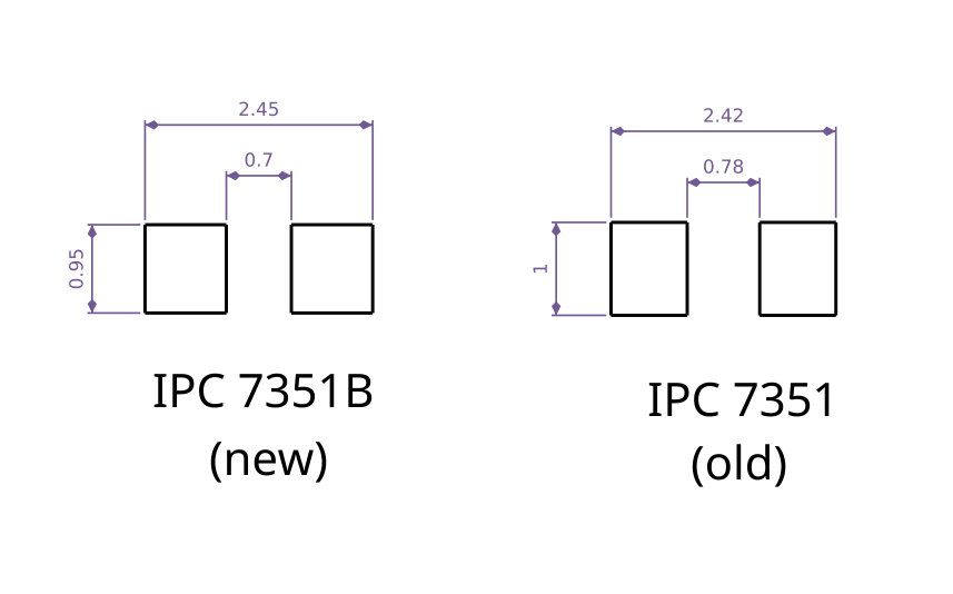
I will still update the footprints to use IPC-7351B as it is newer than the standard originally used.

The differences between the IPC-7351 and IPC-7351B are as follows:
For square end < 0603 (nominal density):

  • Toe old = 0.1, new 0.2
  • Heel old = -0.05, new 0.0
  • Side unchanged at 0.0
  • Courtyard unchanged at 0.15
  • rounding base is now 0.02 for all measurements. (Was 0.05)

For square end >= 0603 (nominal density):

  • Toe unchanged at 0.35
  • Heel old = -0.05, new 0.0
  • Side unchanged at 0.0
  • Courtyard unchanged at 0.25
  • rounding base is now 0.05 for all measurements. (Was 0.02 for heel and toe direction and 0.1 for side direction)

Edit: this is the resulting difference for the 0603 footprint:
screenshot from 2018-06-07 22-03-06

@myfreescalewebpage myfreescalewebpage added Abandoned Original author has stopped working on the PR Enhancement Improves existing footprint in the library labels May 14, 2020
Sign up for free to subscribe to this conversation on GitHub. Already have an account? Sign in.
Labels
Abandoned Original author has stopped working on the PR Enhancement Improves existing footprint in the library
Projects
None yet
Development

Successfully merging this pull request may close these issues.

5 participants